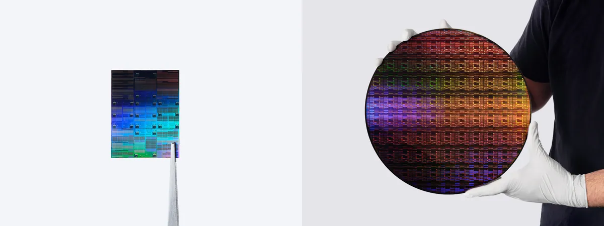
IBM demonstrates 0.7nm transistors at Albany, with Tokyo Electron and SCREEN as research partners
IBM's Albany research consortium — including Tokyo Electron and SCREEN Semiconductor Solutions — has demonstrated functional CMOS inverters at 0.7nm (7 angstroms), using a nanostack architecture that stacks transistors vertically to roughly double the density of its 2nm node. Production is approximately five years out, but the work confirms angstrom-era scaling is physically achievable, and Japan's two major equipment suppliers co-developed this IP alongside IBM — not as downstream licensees.
Source: newsroom.ibm.com ↗
With the new nanostack architecture, logic technology can extend for the first time below the 1 nm node, advancing the era of angstrom-level scaling, where dimensions approach the size of individual atoms.
IBM Research
Why this matters
- → Breaks through physical scaling limits; confirms atomic-scale transistor density gains possible
- → Doubles chip density vs. 2nm; enables 50% more performance or 70% better efficiency
- → Japanese equipment makers (TEL, SCREEN) co-developed IP, not just licensed downstream tech
Atoms become transistors